| Description |
|
Electron microscopy analysis — which includes transmission electron microscopy (TEM) with energy-dispersive X-ray analysis (EDX), and scanning electron microscopy (SEM) with EDX — can provide direct observation of microstructural features on a surface, at an interface, and inside a bulk material. At EMSL Analytical, our instrumentation (3 TEMs and 3 SEMs, precision ion polisher, and cryo-ultramicrotome) and staff expertise in electron microscopy enable us to provide quick turnaround service.
|
 Dislocation networks in NiAl single crystals Dislocation networks in NiAl single crystals |
TEM can be an appropriate choice for crystalline defect analysis. Knowledge of crystalline defects is important in predicting behavior and finding failure mechanisms for metallic and electronic materials. Defects such as voids, stacking faults, dislocations and loops can be revealed and analyzed using weak beam dark imaging, trace analysis, and other techniques.
|
|
TEM analysis can also be used in applications such as nanoparticle size distribution, phase transitions and strengthening mechanisms in metallic and ceramic materials, structure of polymers, identification of precipitates and dispersive particles, phase orientation relationships, and thin film analysis.
|
|
An even wider range of applications utilizes SEM, partly because of the ease and lessdestructive nature of sample preparation. A few examples of SEM/EDX services include the identification of particles, fracture surface analysis, analysis of coatings, patterning and defect characterization of microelectronic devices, and elemental distribution analysis.
|

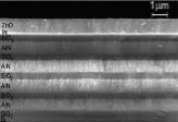
SEM cross-section image of a zinc oxide-based thin film resonator (TFR) used as front-end filter in wireless communication systems
|
|
 Order Sampling Supplies
 Request Pricing
 Technical Questions
 24/7 Account Access
 Email Us


